
FAQ
Diode FAQ
Can I operate the recommended MD90 F18 and MD90U25 replacements without over potting them?
The recommended replacement for the MD90F18 is the SXF20FF3. The recommended replacement for the MD90U25 is the SXF6523. If the diodes are operated at full rated voltage, the voltage stressed between leads will exceed the general design guideline of 10V/mil in air. It is recommended that the isolation voltage between leads be increased through the use of a conformal coating, the use of a dielectric liquid or vapor.
Can I operate an axial-leaded 10KV diode without it arcing from lead-to-lead?
A rule-of-thumb for determining whether additional encapsulation is required is the 10KV/inch isolation in air rule, which assumes relatively low humidity and clean air (no particulates on the diode). For example, using the 10kV/inch rule for the 1N6517 diode (5kV, 1A, 70ns), based on body size and distance between leads, it could operate up to 2900V in clean, dry air. Above 2900V, or in less clean conditions, the diode should be encapsulated or operated in oil or some other dielectric fluid.
Many factors can effect whether the 10KV/inch rule is effective in applications. Additional factors include humidity levels, thickness of the glass passivation, body length between leads, ambient temperatures, vacuum levels, and power levels.
Generally speaking, additional isolation should be provided for diodes operating a levels of 5KV or higher.
Can diodes be matched for Trr?
Occasionally in high frequency applications where voltage rise times are fast, matching Trr can be advantageous. This only works for single junction diodes (1KV or less). Individual junctions in high voltage multi-junction diodes (greater than 1KV) cannot be accessed.
Multi-junction diodes work very well in high frequency applications.
Do VMI diodes have a hard or soft recovery time (Trr)?
Soft recovery.
Do VMI diodes have avalanche capability?
Yes and no. 100% of our diodes are tested under avalanche conditions at 100uA. Yes, all of our diodes have some avalanche capability.
The real question becomes, “How much?” That varies from diode to diode and depends on several factors including number of junctions, junction area, resistivity of the wafers, the energy or power dissipated, and more.
In avalanche mode, a diode is reverse biased. Leakage current increases exponentially as the reverse voltage increases. Dissipated power increases as leakage current increases, which heats up the diode junction. Heating up the diode junction increases the leakage current, which increases the dissipated power, and so on until the diode fails catastrophically. If the diode is kept cool, it will continue to operate indefinitely.
VMI diodes are tested in such a way as to ensure reverse leakage current is low enough at the rated PIV to help prevent thermal runaway commonly associated with avalanche mode operation.
If the customer knows what the avalanche requirement is, VMI can determine if the diode in mind will meet it.
Is it possible to connect diodes in series to increase reverse voltage capability? Is it possible to connect them in parallel to increase the forward current?
Yes. Diodes can be connected in series and/or parallel in order to increase the reverse voltage and/or forward current capacities.
There are practical considerations to keep in mind such as thermal management, voltage isolation, and component count, to name a few.
When connecting diodes in parallel it is usually a good idea to match Vf. Differences in Vf between diodes will get worse as they heat up. Diodes with lower Vf will initially conduct more current, increasing their power dissipation and further lowering their Vf. This in turn increases their current share, continuing to heat up the junction, and so on until a catastrophic failure occurs.
What is the (I2)T rating and how is it used?
The I2T (Amps2*Seconds) rating is defined as the single cycle surge current, Ifsm, multiplied by a standard pulse width of 8.3mS (sine wave is assumed).
It is used as a rule-of-thumb to gauge surge capability at different pulse widths. It works because at higher currents, Vf (forward voltage drop), is dependent on the resistive element of the diode. Vf becomes proportional to current in the diode expressed by Vf = Rdiode * If. The I2T calculation yields energy dissipated in the diode during the pulse duration. Power multiplied by pulse time gives the energy pulse. Energy dissipated during a surge current pulse is proportional to I2T and is usually the driving force behind a failure. The energy pulse causes localized heating which induces mechanical fractures or disruption of the silicon crystal structure. Calculating the maximum I2T can help determine if a diode will survive a current surge.
Example: A diode has an Ifsm rating 100A. Will it work at 150A surge for 1uS?
Solution:
1. Calculate I2T
I2T = (100A)2 * 8.3mS = 83A2S
2. Determine if I2T under the new conditions is much less than the original calculation. Is the I2t calculation at 150A, 1uS much less than 83A2S?
Is 83A2S >> (150A)2*1uS?
= .023 A2S
Yes, .023A2S is << 83A2S
The diode should be able to handle a surge of 150A for 1uS.
Comment: When approaching fast pulse times (i.e. ns range), I2T using Ifsm is used as an upper limit. Operating I2t should not exceed half of the upper limit.
Will plastic diodes work in high temperature down-hole applications?
Plastic diodes have very high leakage current at extended high temperature, and are not recommended for the HT options.
I am trying to determine the polarity of a high voltage diode. My Fluke meter shows an open circuit in both directions for the 10KV Z100UFG diode. Is that normal?
Yes, and no. When trying to identify the cathode and anode end of a high voltage diode, the meter has to have enough voltage to overcome the forward voltage drop, Vf, of the device under test. We use a test setup that includes a 30V current limited power supply. When testing for polarity, the current should be limited to mA going through the diode when it is connected in the forward direction.
What is the most effective way to mount the K25UF epoxy diode to a printed circuit board?
The most effective method of mounting the K25UF diode (and most all axial-leaded epoxy diodes) is to make a cut-out in the board just a tad larger than the dimensions of the diode body and drop the diode in so the leads lay flat across the solder pads. If possible, avoid lead-forming. If space does not permit it, is important to support the diode body while forming the leads. The leads are relatively short and thick, which enhances the current carrying capacity of the device. The epoxy body is easily damaged if the leads are not supported near the body during the lead forming process.
Does VMI manufacture space-level diodes?
The highest level QPL diode VMI manufactures is JANTXV. We have on many occasions, “up-screened” JANTXV diodes to the space level by following testing and processing guidelines outlined by NASA. Please contact us if you are interested in space level diodes.
Do you have any info on the failure rate (FIT rate) @55C and @60%CL for the MD90FF18J based on in-house life test data?
VMI does not have any in-house life test data, but the calculated MTBF (Mean Time Between Failure)at 55C and operating 60% in a stressful environment (Missile Launch conditions) is 43 years.
If you have questions about MTBF on specific diodes, please contact us.
Is the dimensional information on the diode spec sheets nominal numbers, or maximums? If they are nominal, what are the maximum and minimum ranges for the packages VMI manufacture space-level diodes?
When diodes are used in a bridge or string configuration is it necessary to place equalizing resistors across the diodes? Also, is it necessary to place capacitors in parallel with the equalizing resistors to reduce noise and high voltage spikes?
Balancing resistors and capacitors are generally not required when using VMI diodes. A resistors connected in parallel with a rectifier is intended to balance the reverse bias voltage across the series rectifiers. As such, the resistor value needs to be selected such that the current through the resistor is fairly large compared to the reverse leakage of the diode, thereby making a stiff divider circuit. If there are relatively high leakage currents expected in the diode, this can result in a significant power loss in the balancing resistors.
Capacitors connected in parallel to resistors/diodes can be used to balance voltages across diodes during transient conditions, or ringing. Care must be taken to select the capacitors small enough so as not to impact the rectified waveform at the output of the diode.
VMI’s diodes are well-balanced for Ir and reverse recovery time (Trr).
Many of VMI’s diodes have up to twenty junctions in series. The series junctions operate under many kinds of applications, and all sorts of conditions without compensating resistors or capacitors with no problems.
What are the maximum storage and operating temperatures for silicon diodes?
Are overmolded diodes (SMF, SXF families) hermetically sealed?
Answer: The SMF and SXF families start with the basic, glass-body, hermetically sealed diode, and over mold it in a rigid epoxy. Following the encapsulation process, the leads are trimmed and formed. The diode itself is hermetically sealed. The epoxy is extremely moisture resistant, but not water-proof.
Some rectifier assemblies show Io, forward current in air, or oil. What do the ratings mean?
Frequently the current rating, Io, of a rectifier assembly contains the following info:
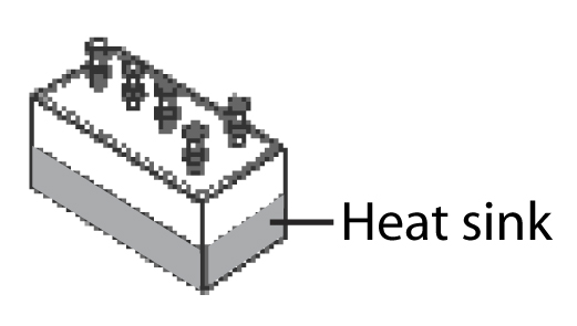
A typical rating might include –
- Io, 70°C in oil
- Io, 55°C heat sink
- Io, 25°C no heat sink
The current rating in oil assumes 70°C is the temperature of the oil, and that the oil is circulating.
A temperature of 55°C assumes that is the temperature measured at the bottom of the heat sink, opposite the site of attachment to the assembly.
An ambient temperature of 25°C assumes that is the temperature of the air, not the case temperature.
Multiplier FAQ
Do the MVM series multipliers come in a negative Vout version?
The MVM series can be used to generate either a positive or negative output voltage.
- To get a negative output voltage from the MVM type series, connect your input signal to V2. The HV output will be V1, and the output voltage will be negative.
How does temperature effect the output of the MVM302P08 hybrid multiplier?
Keeping all things constant, the output voltage decreases as the temperature increases. There is a significant drop-off at temperatures higher than 150C. Other factors effecting output voltage include load current and operating frequency.
Other hybrid families exhibit the same phenomena. The actual output voltage varies depending partly on the number of stages and input voltage. Other factors include operating frequency, output current, and type of load.
Will a multiplier work at an operating frequency of 60Hz?
No. Most multipliers work best between 25KHz and 150KHz. There are exceptions to the rule, but generally the absolute minimum operating frequency is 10KHz.
Operating frequency directly impacts
- Ripple voltage (the higher the operating frequency, the lower the ripple voltage)
- Regulation voltage (the higher the operating frequency, the less drop in output voltage at load)
Higher operating frequencies have greater efficiency in the multiplier. For a slow 60hz signal, very large capacitances would be required to regulate the voltage properly and have a consistent high voltage output.
Do you make space-level multipliers?
HVP Series Power Supply FAQ
Can high voltage transients interfere with data or signal lines through the voltage or current monitor signals?
The signal lines include interface filtering and suppression components designed to protect the signal integrity and internal components. If an arc occurs during operation, transients can be coupled into the signal lines. Using good grounding techniques as well as shielding the interface cable will normally be sufficient to reduce coupled transients to non-disruptive levels.
What are the cable & connector ratings of the cable provided with the HVP?
The high voltage cable is an option that is purchased separately. The optional cable is rated to 150kV maximum voltage. The connector is a standard Amphenol series 97 circular connector without the pin plug. The connector is used as a shield ground path to the supply frame for the high voltage cable.
What kind of protection systems does the HVP have?
There are three main protection systems –
- Over-voltage
- Over-current
- Arc/short-circuit
Over-voltage System: This circuit limits the voltage output of the high voltage transformer to approximately 110% of the rated output.
Over-current System: This circuit limits the output current of the high voltage transformer using a current sense transformer output compared to a preset reference.
Arc/short-circuit System: This protection encompasses a variety of circuits and components working together to protect the internal components from transient effects of an arc as well as to clamp the output current to the current regulation set value in the event of a short circuit condition.
What are power ratings of the HVP series?
The HVP series power supplies are 250W supplies. They are available as either a positive or negative output as follows:
- 50kV 5mA
- 80kV 3mA
- 125kV 2mA
LP6 HeNe Laser Power Supply FAQ
How does the Run Current effect the Run Voltage?
The LP6 series is rated for 6W maximum output. The Run Current is preset at the factory, and can range between 2mA and 5mA. The Run Voltage is determined by dividing the maximum output power by the Run Current.
For example if a Run Current of 3mA is specified (by the customer), the Run Voltage will be (6W) / (3mA) = 2000V
Once the Run Current is set, it cannot be changed – i.e. it is not “adjustable” by the customer.
XRS Series Portable X-Ray Power Supply FAQ
Will the power supply be damaged if pins 7 and 8 are accidently reversed?
There should be no damage.
What is the impedance of pins 7, 8, 9, and 10?
Pin 7: 11k ohm
Pin 8: 100kohm during normal operation
Pin 9 and Pin 10: 10k ohm
Is there any protection on the pins?
All interface pins have protective diodes and series resistors.
Optocouplers FAQ
What kind of processing is available?
Processing should be specified by the customer and reviewed by engineering. Most processing should be done on the final assembly. Diode processing is limited due to requirements for use in an onto coupler.
Are custom configurations available? If so, what are the costs and how long will it take?
Custom electrical configurations are not available.
Custom mechanical changes to the lead configuration or package size will require a new mold (upwards of $10K) for the OC-100 style, and a new shell for the OC-250 style.
The packages can only increase in size.
Custom mechanical changes can take upwards of twenty weeks depending on vendors, yields, and schedules.
Can the package styles be made smaller?
No. The package sizes have been optimized to accommodate the various LEDs and photo diodes.
Can the potting material be changed?
No. The potting material has been specially selected to maximize the optical transmission of light from the LED to the photocopies.
Do I have to run the photo diode at 10KV or 25KV?
No. The 10KV rating for the OC-100 and the 25KV for the OC-250 are maximum ratings.
Do both of the LEDs in the OC-100 family have to be working in order to get an output from the photo diode?
No, but the output (Ir) of the photo diode is decreased by one half if only one LED is working.
Can the LED current range be increased?
No. The manufacturer of the LED determines the LED current range. The end user must not exceed the maximum current as specified by the manufacturer.
Is the Vf rating for the LED for the whole assembly, or for each LED?
The Vf rating is for each LED shown on the schematic.
What is the forward current (If) range through the OC-100 LED? What about current through the OC025?
For the OC-100 family, each LED is rated at 100mA.
For the OC025 (2.5kV opto-coupler), the rated If of 50mA, is for a single LED. VMI recommends that all four LEDs are connected in series so each LED sees the same amount of current.
What is the minimum gain of the OC-100 family devices?
Gain is determined by output/input, and in this case, is also dependent on the level of applied reverse voltage. Defining “gain” as LED current/Optocoupler current, the following graph illustrates gain at two different levels of Vrwm.
For example, at Vrwm = 1KV, and I(LED) = 30mA, Gain = .00077 = (23uA)/(30mA). Similarly, at Vrwm = 4KV, and I(LED) = 30mA, Gain = .00087 = (26uA)/(30mA)
What is the power gain of the OC-100 family devices?
The power gain is 2. This is the ratio of the output power of the photo diode divided by the input power to the LEDs.
PTR = (10KV x 100mA) = 1
(5V x 100mA) .5
1/.5 = 2
Can the current gain be increased?
No. The current gain is fixed.
What is the current gain of the device?
The current gain of the device is 1/1000. This is the ratio of the output current (diode leakage current) divided by the forward current through the LED(s).
CTR = 100mA = 10E-06 =. 001 = .1%.
100mA 10E-03
Does the gain change with temperature?
Gain changes over temperature. Gain decrease as temperature increases. It is linear over the temperature range of –25C to +150C.
VMI provides a graph of Gain vs. Temperature as part of the data sheet.
Is it possible to get a 2W 10KV opto-coupler in the OC-100 style package?
In order to build a 2W opto-coupler, the number of LED’s would have to double, and there would have to be a way to remove the heat from the high voltage diode. It is not possible to do all of that and keep the package size the same.
However, it is possible to connect two OC-100 style optocouplers in parallel to get the equivalent of a 2W device.
Is it okay to put two 25KV OC-250 opto-couplers in series to get a 50KV opto-coupler?
Is it okay to put two OC-250, or OC-100HGs in parallel?
Is the OC100HG opto-coupler RoHS compliant?
I recently installed six optocouplers in a two-channel push-pull circuit. I checked the LEDs with an near-infrared viewer before applying high voltage and noticed there s a lot of light coming out of the clear housings. It seemed like a significant amount, compared to ambient light. Will painting the outside of the devices black, or wrapping them in electrical tape cause problems? (electrical breakdown). The concern is the potential for optical cross-talk while operating at 6kV preventing the “off” arm from completing turning off. I also noticed that there are two small holes in the housing (not near any leads) Do these need to be left uncovered?
Cross-talk can be an issue with these devices. Because they are high voltage, many end-users will encapsulate the optocouplers (and surrounding circuitry) with an epoxy or coating to further insulate the optocouplers. This epoxy is usually opaque, so it eliminates the cross-talk.
You can paint or otherwise coat and protect the optocouplers, but you will want to do some testing after the parts are coated to ensure the coating does not cause any arcing around the part at your applied voltage levels. Some customers paint the outside of optocouplers with a white paint to have more complete internal reflection in the optocoupler, increasing the gain of the device.
The two holes you mentioned are just depressions in the epoxy that are there to assist in centering the LEDs during molding. They are not significant to the operation of the optocoupler. They can be covered up if you like.
What is the impact of ambient light on the opto-coupler?
What is the thermal resistance of the module to air?
What is the turn-on time between the voltage applied to the photo diode and turn-on of the opto-coupler?
The delay time between the LED current and reaction time of the photo diode is listed as 2µs in the data sheet. It is defined as Ton and Toff.
Of more concern is the capacitive load. The output current supplied by the photo-diode is dependent on the LED current, and the gain of the opto-coupler (refer to data sheet). The opto-coupler acts like a current source. The switching time will depend on how long it takes the current output from the opto-coupler to charge the load capacitance.
What is the long term gain degradation?
Over time the gain on the OC100HG will decrease as rapidly as 30% over a three-hour time frame when running both LEDs at the full rated current of 100mA.
Lower operating levels of LED current results in a slower decline in opto-coupler gain, but a gain drop has been observed in even very low LED current levels over time.
Solution – MI suggests using the OC100G opto-coupler as a replacement. Gain degradation in the OC100G is less severe over time, but the initial gain is less than that of the OC100HG. Coming Soon – Comparative Gain Degradation Graph
Recommended Replacement – We recommend the as a replacement for applications that do not require high gain.